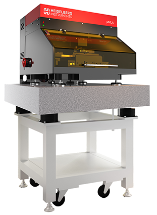
Maskless lithography means that your design file is exposed directly onto the resist-coated wafer. The production of a photomask is not required.
Maximum substrate size: 6” X 6”
Minimum substrate size: 5 X 5 mm²
Maximum write area: 100 X 100 mm²
10mm maximum substrate thickness
Substrate thickness: 0.1 to 12 mm
Minimum feature size of 1 μm
